
Blog
Search for the insights
11/09/2026
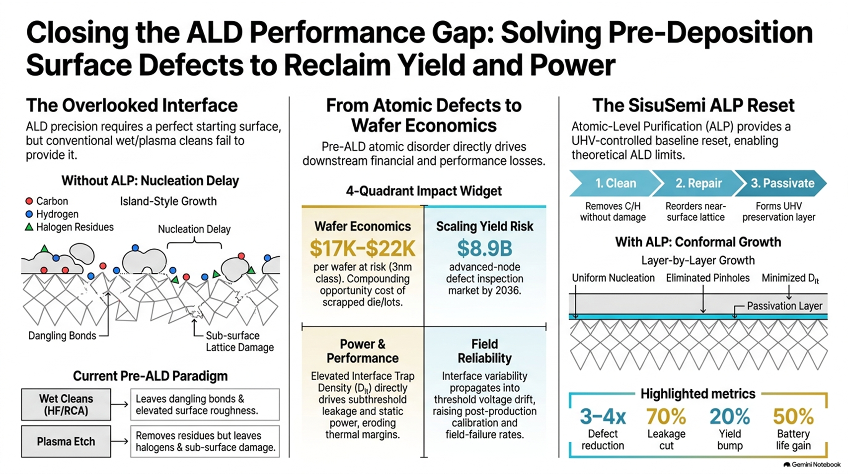
When the Foundation Cracks: How Pre-ALD Surface Defects Undermine Atomic Layer Deposition
Atomic Layer Deposition has earned its place as the workhorse of advanced-node manufacturing. Its self-limiting, layer-by-layer chemistry gives fabs something no other deposition method can
Read More →
04/09/2026
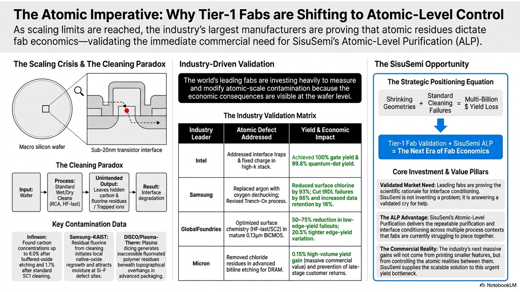
The Industry Is Looking Deeper: Why Atomic-Level Defects and Contamination Have Become a Strategic Semiconductor Priority
For decades, semiconductor manufacturing progress was described mainly through lithography, transistor dimensions and wafer-scale yield. The research papers reviewed here show that the industry’s attention
Read More →
28/08/2026
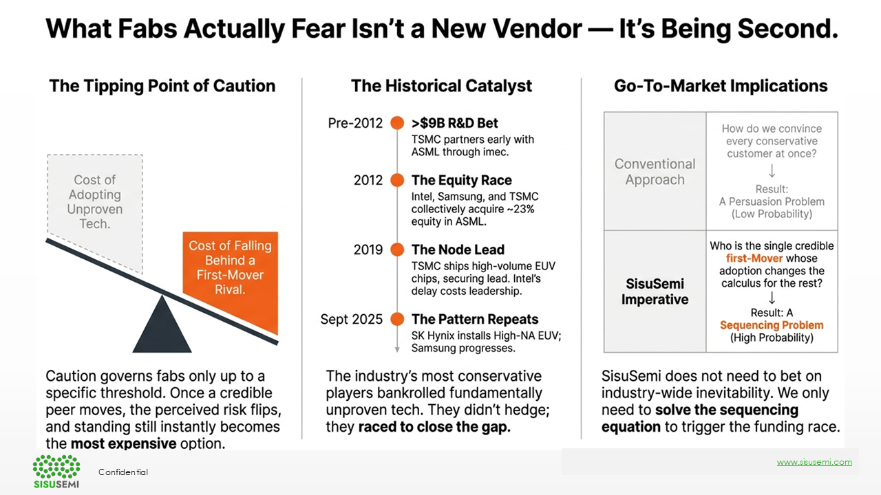
What Fabs Actually Fear Isn’t a New Vendor – It’s Being Second
The typical assumption about semiconductor manufacturers is that they’re conservative almost by temperament: risk-averse, slow to change, unwilling to bet a production line on anything
Read More →
21/08/2026
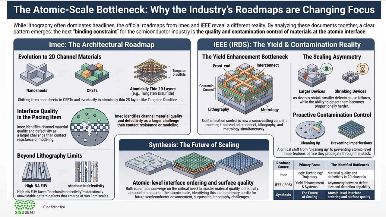
What the Public Roadmaps Signal About the Next Atomic-Scale Bottleneck
Roadmaps are the least hyped documents in the semiconductor industry, which is exactly what makes them worth reading closely. Nobody is trying to raise money
Read More →
14/08/2026
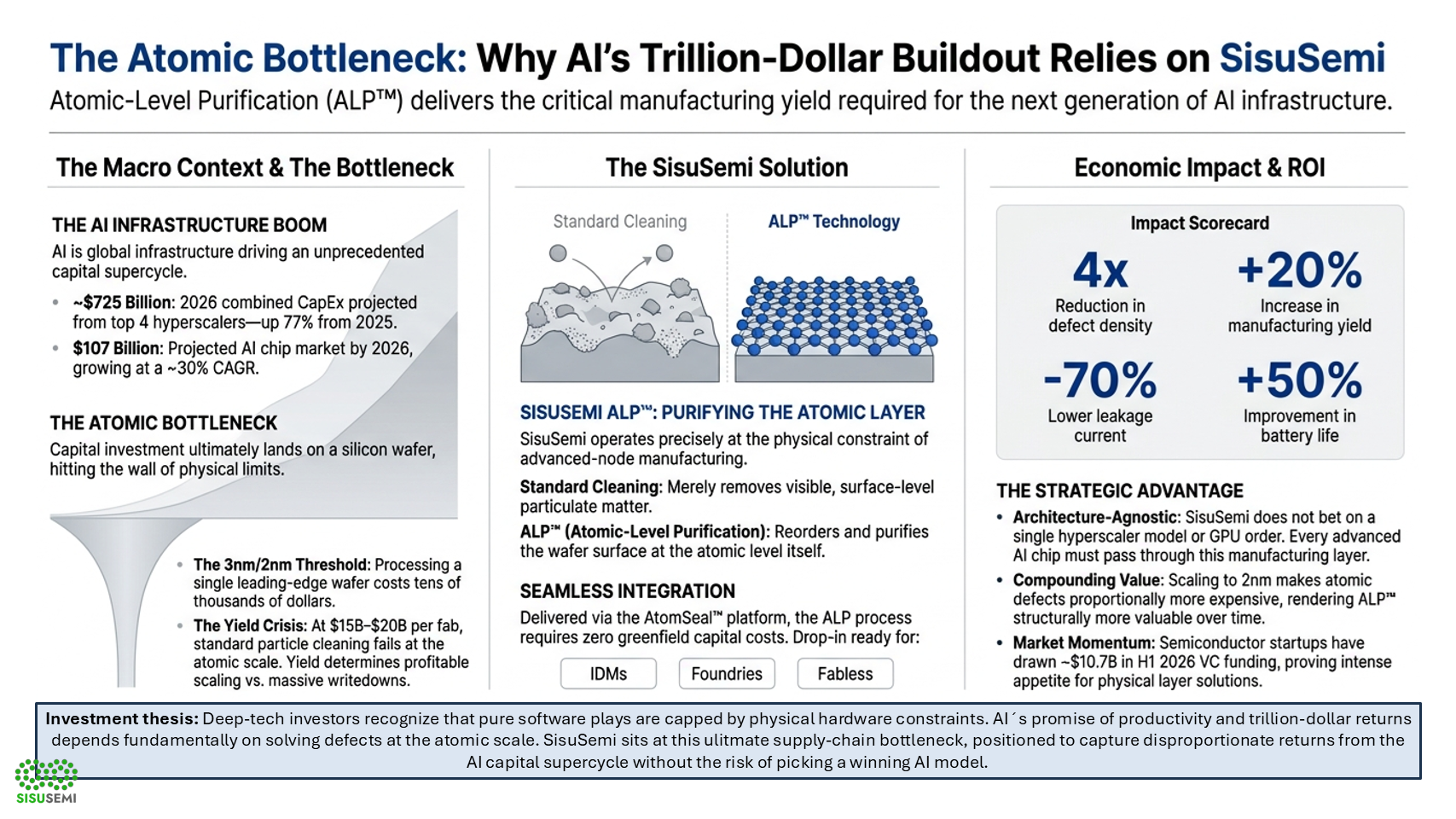
The Atomic Bottleneck: Why AI’s Trillion-Dollar Bet Runs Through Semiconductor Purity
Artificial intelligence has stopped being a demo and become infrastructure. In under three years, models like ChatGPT, Claude and Gemini have moved from research curiosities
Read More →
03/07/2026
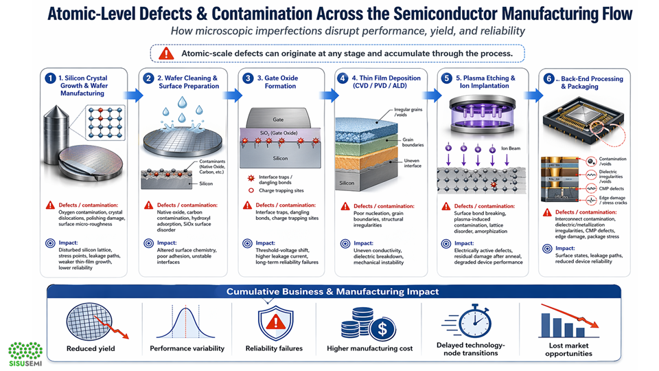
Atomic-Level Defects and Contamination in Semiconductor Manufacturing: Challenges, Business Impact and Future Opportunities
Semiconductor manufacturing is one of the most precise industrial processes ever developed. Modern chips are fabricated at nanometer scales where even a single misplaced atom
Read More →

26/06/2026
Oxide-Free Interfaces: The Problem No One Sees But Everyone Pays For
Modern semiconductor manufacturing assumes that a clean silicon surface is “good enough” after standard HF-last processing. In reality, this is not the case. After the
Read More →
05/06/2026
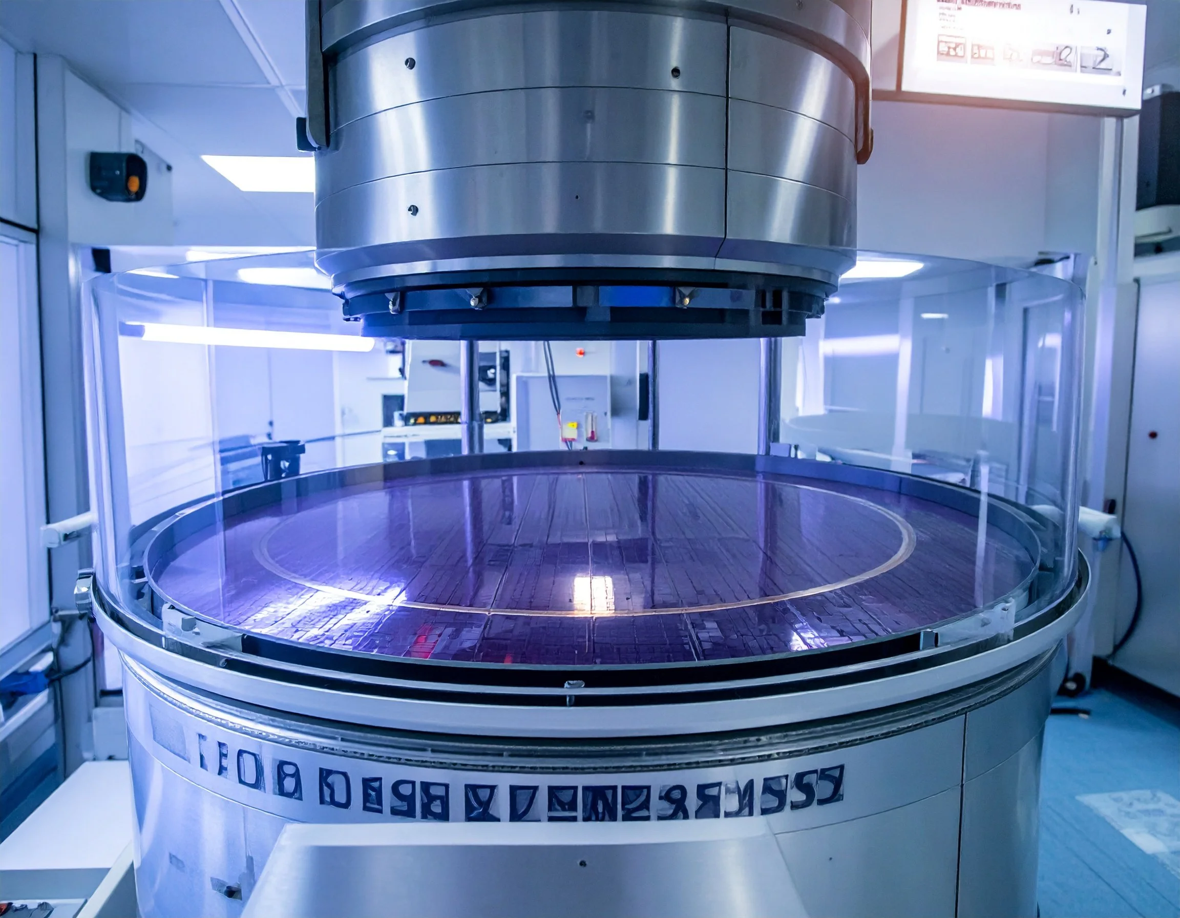
Bridging the Gap: Overcoming Atomic-Level Challenges in Heterogeneous Integration
In the pursuit of More-than-Moore scaling, wafer bonding has emerged as a cornerstone of heterogeneous integration. By enabling the fusion of disparate materials—such as GaN-on-Silicon
Read More →

22/05/2026
When Every Atom Counts: How Atomic-Level Defects Are Redefining MOSCap Performance — and the Business Case for Solving Them
For decades, the semiconductor industry managed defects the way you manage visible dirt: with progressively finer filters, cleaner rooms and tighter process controls aimed at
Read More →
15/05/2026
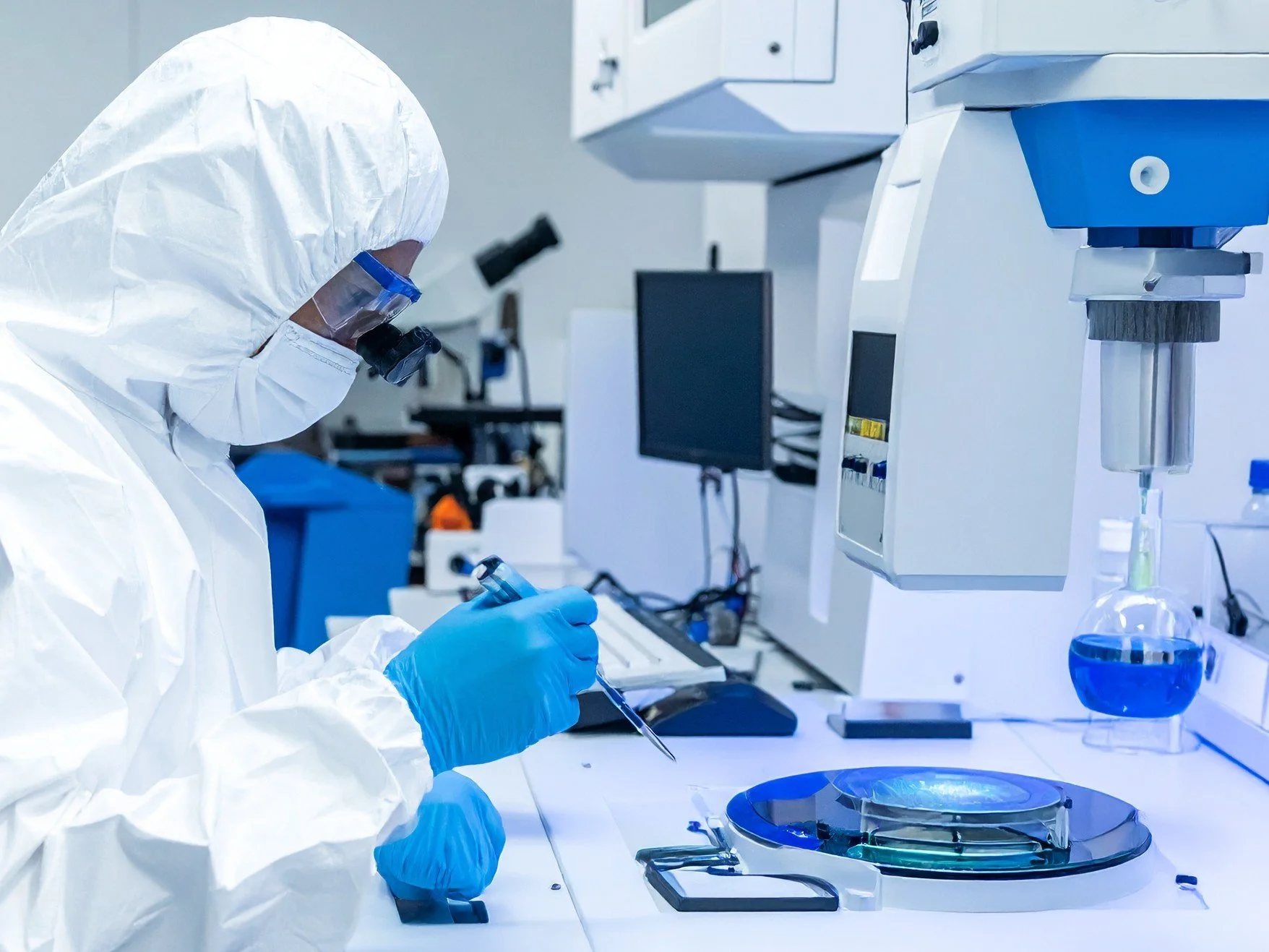
Atomic-Level Defects in FETs: An Invisible Challenge in Modern Semiconductor Manufacturing
Field-effect transistors (FETs) are the fundamental building blocks of modern electronics, enabling everything from mobile devices and automotive systems to advanced computing and communications. As
Read More →